|
<< Click to Display Table of Contents > Digital Input And External 5 V Supply |
  
|
|
<< Click to Display Table of Contents > Digital Input And External 5 V Supply |
|
The signals, applied to the Digital Inputs, are transmitted to the USC-2 via the Status wires of the XY2-100 interface. Figure 7 shows the pin assignment of the digital input connector JP1. The applied high level voltage should be in the range of 2.1 V to 15.0 V.
|
This feature can only be used in combination with the USC-2. |
|---|
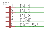
Figure 8: JP1 - Digital input connector pin assignment
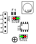
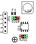
JP1 also provides the pins for the optional external 5 V power supply. Therefore pin 4 is used as GND and pin 5 is used for the 5 V. The solder jumpers SJ10 and SJ11 are used to choose between internal or external supply. The jumper positions are shown in the figures 9 and 10.
|
Green means closed and red means open. The default configuration is internal 5 V supply. |
|---|
Figure 9: Internal 5 V supply |
Figure 10: External 5 V supply |
|---|